mainmenu
- About Center
- Members
- Research
- Publications
- Facilities
- Super-depth Optical Imaging Lab
- Ultrafast Infrared Spectroscopy Lab
- Ultrafast IR-Visible Spectroscopy Lab
- Instrument and Chemistry Lab
- Molecular Imaging Lab
- Multidimensional Infrared Spectroscopy Lab
- Sample Preparation Lab
- Optical Frequency Comb Spectroscopy Lab
- Single Molecule Imaging Lab
- Spectroscopic Imaging Lab
- Theory and Computation
- Open Access Facility
- Collaborative Research Equipment
- Quantum Spectroscopy Lab
- Ultrafast Raman Probe Spectroscopy Lab
- Equipment Inventory
- Board
Board
News
IBS create a multi-channel nano-optical device dramatically increasing the parallel processing speed of microprocessors
IBS create a multi-channel nano-optical device dramatically increasing the parallel processing speed of microprocessors
- Researchers from the Center for Molecular Spectroscopy and Dynamics (CMSD) increase the number of communication channels -
Microprocessors play a pivotal role in computers and have steadily increased the speed of information processing over the past several decades. However, due to technical limitations such as heat generation due to integration, the processing speed of semiconductors has remained at several gigahertz (GHz) for the past decade. As a current alternative to this, many microprocessors are used in parallel, but the electrical connection between the processors is slow, creating a bottleneck for data transfer. To solve this problem, many studies have been conducted to merge processors by using optical signals which are several hundred times faster than electrical signals.
CHOI Wonshik, Associate Director of the CMSD, lead the research team that created an innovative device. The team discarded with the conventional method of periodically arranging the nano antennas. Instead, they devised disordered arrangement of the antennas to minimize redundancy between the antennas and enabled each antenna to function independently. As a result, the device can provide 40 times wider bandwidth than existing antennas periodically arranged. "We are proposing a new way to connect nanoscale microprocessors to ultra-high-speed optical communications," commented Dr. Choi. The research will appear in the March edition of Nature Communications.

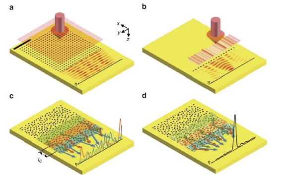
▲ Numerical and theoretical analyses describing the performance of a 2D disordered array of nanoholes in channel transfer form far-field input to SPP output.*
* a) A 2D array of periodic nanoholes patterned on a metal film. Black dots indicate the positions of the holes. SPPs generated by a normally incident plane wave propagates along y-direction. Scale bar, 2 mm. (b) A 1D array of nanoholes patterned on a metal film. The incident wave whose wavefront is properly shaped focuses the SPPs generated at the nanoholes at a target spot on a sampling line (Z). (c) A 2D array of disordered nanoholes patterned on a metal film. Ordinary planar incident waves generate speckled SPPs. The blue, red and green curves at the sampling line are the SPP fields originating from the representative far-field illumination of the blue, red and green rectangular areas, respectively. The wavelength of the light source was 620 nm. The SPPs were uncorrelated if the centre-to-centre distance between two neighbouring illuminations was larger than the characteristic length lc described in the main text. (d) The same pattern of nanoholes as (c), but the correct choice of wavefront for the illuminations at the blue, red and green rectangular areas can cause the SPPs to constructively interfere at the target point (black curve). All the results displayed here were derived from the numerical simulations using the finite-difference time-domain (FDTD) method (see Supplementary Note 1 for details). (e) Expected enhancement factor for channel number.
The team used surface plasmons to mediate optoelectronic signaling. At nano antennas, optical signals are converted to surface plasmons, which then propagate through metal surface as electric signals. The researchers randomly arranged the nano antennas, and the surface plasmons generated at each antenna underwent multiple scattering to minimize redundancy between the antennas. In this way, each of the antennas can be used independently, resulting in a substantial increase in the effective number of antennas to more than 40 times. An increase in the number of antennas means an increase in the number of multiple input channels in the MIMO communication, which leads to an increase in the information transmission bandwidth.

▲ Expected enhancement factor for channel number.
To exploit the benefit of disordered arrangement of antennas, the team had to resolve an innate problem. Random multiple scattering by disorderly arranged nano antennas is unpredictable, and cannot be used for information transfer without special measure. The researchers analyzed the patterns of multiple-scattered surface plasmons for various optical inputs and found a particular optical input signal that could send the desired signal to a particular microprocessor. The spatial light modulator was used to generate the identified optical input signal, and the surface plasmon could be controlled freely. "Using this," offered Doctor Choi. "We proved that we can transmit signals to six different microprocessors at the same time and proved that optical images are converted into plasmons."
Neil Mannix
Notes for editors
- References
Wonjun Choi, Yonghyeon Jo, Joonmo Ahn, Eunsung Seo, Q-Han Park, Young Min Jhon & Wonshik Choi. Control of Randomly Scattered Surface Plasmon Polaritons for Multiple-input and Multiple-output Plasmonic Switching Devices. Nature Communications (2017). DOI: 10.1038/ncomms14636
- Media Contact
For further information or to request media assistance, please contact: Mr. Shi Bo Shim, Head of Department of Communications, Institute for Basic Science (+82-42-878-8189, sibo@ibs.re.kr); Ms. Carol Kim, Global Officer, Department of Communications, Institute for Basic Science (+82-42-878-8133, clitie620@ibs.re.kr); or Dr. Letizia Diamante, Science Writer and Visual Producer (+82-42-878-8260, letizia@ibs.re.kr).
- About the Institute for Basic Science (IBS)
IBS was founded in 2011 by the government of the Republic of Korea with the sole purpose of driving forward the development of basic science in South Korea. IBS has launched 28 research centers as of January 2017. There are nine physics, one mathematics, six chemistry, eight life science, one earth science and three interdisciplinary research centers.

